Clarity 3D Solver
A solution for modeling the electromagnetic properties of printed circuit boards, microcircuit substrates and connectors in 3D with unparalleled speed and accuracy.
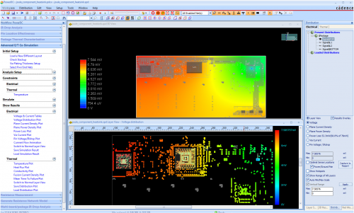
Cadence has announced a new program for analyzing the electromagnetic properties of printed circuit boards and IC substrates in 3D – Clarity™ 3D Solver. This simulator uses the finite element method (FEM), dividing the spatial model of the information transmission channel into many micro-tetrahedra and solving the Maxwell equations on the faces of these elements. A unique algorithm for parallelizing calculations across multiple processors and servers allows up to 10 times faster problem solving compared to traditional simulators.
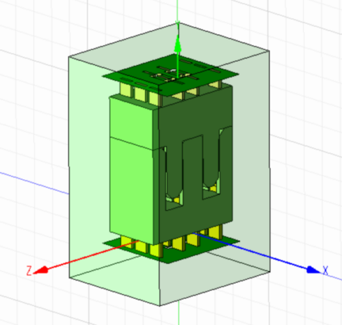
Clarity obtains complete information about the package design and PCB layout from CAD tools, including from CAD designs of printed circuit boards or Cadence Allegro, OrCAD, SiP chip substrates. Moreover, Celsius can obtain information on the detailed design of the connectors connecting the board and the IC substrate, as well as the wires used in IC chip desoldering, and BGA and FlipChip balls. Domestic developers of processor microcircuits who use Cadence CAD for designing VLSI and packages / substrates of microcircuits may be interested in this functionality (CAD for developing substrates Cadence Allegro Package Designer / System In Package is an extended version of CAD for printed circuit boards Cadence Allegro PCB Designer).
The simulator is easily integrated into Cadence electronics design software. Component topology and PCB geometry are read from Cadence proprietary format files. Neutral file formats such as STEP are used to represent the geometrical parameters of the 3D device design, connectors, and 3D objects on printed circuit boards and components.
More information can be found here.