For Developers
If you are designing electronics as a circuit designer, or a PCB design engineer, or a microwave design specialist, or an FPGA RTL code developer, you will be interested in getting acquainted with the CAD software packages that we offer in the Products section. Most of the products can be tested on your own by ordering a temporary demo license from us, or you can get acquainted with their capabilities at our trainings and webinars.
Our website also publishes news for developers, information and training materials, announcements of upcoming seminars and webinars, videos of previous events.
You might be interested in our blog dedicated to discussing various professional events in electronics.
Sign up for our newsletters to receive up-to-date information and be aware of upcoming events.
Новости для разработчиков

Webinar 27.05.2024: SMT stencil preparation, tips & tricks, and design software
On Monday, May 27 2024, we have successfully provided a webinar on the nuances of PCB surface mount stencil preparation and a demonstration of Stencil Designer software for stencil preparation. Please see the blog post on this topic.

Productronica 2023
Averture was invited by Vayo Technology to take part together in Productronica in Munich. It’s been a pleasure working with you. Warmest congratulations on your achievement!

Evertiq Expo 2023, 25-26.10.2023, Warsaw
We have participated in Evertiq’23, the one of the most important events in electronic indstry of Poland. We have been showing the VAYO DFM solution, which helps the electronics manufacturers to verify the PCB project before production, by checking automatically more than 1500 Design For Manufacturing, Design For Assembly, and Design For Test rules. Great…
Developer Materials

Configurations of CAM350
CAM350-070, Gerber Viewer Bundle Import, view and get information.Formats of import: Gerber (274D, 274X, Fire9000, Barco DPF), NC Drill&Mill (Excellon, Sieb & Meyer), netlist (Universal Importer, IPC-D-356 & 356A), aperture table (Universal Importer).Allows to create Stackup and view PCB in 2D or 3D.Functions: View, Query, Report, Measure. Modules: Import – imports Gerber RS-274XInformation – get…

Key features of OrCAD (video)
Embedded net names 3D STEP-models Fillet and tapered traces Static and dynamic shapes RATS options Embedded net names Step support mapping 3D models Group routing Slide function Fillet and tapered traces Shape connecting Shape generating Static and dynamic shapes Creating shapes and circles in OrCAD 16.6 Check out various options for polygons and circles. Pick…
Interesting posts

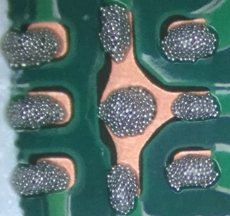
SMT stencil preparation: tips & tricks, and design software
Why do we talk about printing the solder paste and the importance of SMT (surface mount technology) stencil design? Once the PCB layout is finished, the stencil may be the last way we can enhance PCB assembly quality. But currently, stencil design work is typically knowledge-driven, relying on human processes, and can easily cause issues…

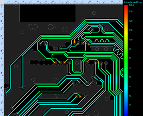
Impedance control issues in PCB manufacturing
Impedance control requirements often accompany the fabrication of complex multilayer printed circuit boards. Understanding the peculiarities of meeting these requirements helps not only to reduce the time for launching boards into production, but also contributes to obtaining a better result. Impedance control at the PCB factory can be roughly divided into several steps: Selection of…

How to make sure that the PCB impedances are correct even after routing changes?
Do you agree that the work of a PCB designer is not always noticeable to others, but very important? The boards you make are built into the latest equipment, often into equipment for responsible use, on which the comfort, health, and sometimes life of people depend. But since these boards are hidden inside the body…
Contact us


