Impedance control issues in PCB manufacturing
Impedance control requirements often accompany the fabrication of complex multilayer printed circuit boards. Understanding the peculiarities of meeting these requirements helps not only to reduce the time for launching boards into production, but also contributes to obtaining a better result.
Impedance control at the PCB factory can be roughly divided into several steps:
- Selection of the structure (if not specified by the customer) and calculation of the refined thicknesses of dielectrics in accordance with the characteristics of the conductive pattern of a particular project;
- Optimal conductors’ parameters calculation in accordance with the structure, actual parameters of the materials used and the requirements for impedances specified by the customer;
- Coordination of calculated data with the designer of the printed circuit board;
- PCB fabrication and testing
If initial data contains information about board structure, the manufacturer selects the closest board structure to the specified from the materials available in the warehouse. If the board structure is not initially specified, then the board structure is selected based on preliminary calculations to provide the smallest deviation of the impedance values actually obtained on the finished board from those specified in the customer’s project. For the selected board structure, a refined calculation of the width of the conductors and gaps is performed, at which the impedance values will be provided most accurately. The board structure formed by the factory and the optimal parameters for the width of the conductors and gaps can be agreed with the developer by e-mail.
The standard accuracy with which factories control impedance is ±10%. In some cases, upon agreement with the factory, the accuracy of the controlled impedance can be increased up to ±7% or even up to ±5%. When designing and manufacturing boards with impedance control, some developers sometimes want to “strictly” meet their specified impedance requirements.
How to choose the best manufacturing option, and will the expectations be true?
The impedance is affected by several factors: conductor parameters, material properties, manufacturing accuracy, internal design features. Let’s try to consider these factors in more detail.
Factors Affecting Impedance
When calculating the refined thicknesses of prepregs in the finished board, the filling of the space between the conductors of the conductive layer, which is determined by the percentage of copper on adjacent conductive layers and the thickness of the foil, should be taken into account. These values used in the calculation should be close to the actual values in the finished board
The percentage of copper on the conductive layer in relation to the area of the board can be calculated using a Gerber-file validation and processing program, such as CAM350 or other programs
The final thickness of the foil in the finished board depends on its starting (base) thickness, as well as on the location – the outer or inner layer in the board structure. For a board that has plated through-holes only (no blind or buried vias and no additional plating steps), the average finished foil thickness can be determined using Table 1.
Table 1. Copper thickness in multilayer PCB layers
| Starting (base) foil thickness, μm | Change in thickness during manufacturing, μm | Average finishing foil thickness | Manufacturing capability example – minimum conductor / gap ** |
| 12 | outer layers ~ +25 | ~ 35 | 3/3mil (0.0762/0.0762 мм) |
| 12 | inner layers up — * | — * | — * |
| 17,5 | outer layers ~ +25 | 43 | 4.5/4mil (0.1143/0.1016 мм) |
| 17,5 | inner layers up -4 | 16 | 3/3mil (0.0762/0.0762 мм) |
| 35 | outer layers ~ +25 | 60 | 5/4mil (0.127/0.1016 мм) |
| 35 | inner layers up -6 | 32 | 3/3,5mil (0.0762/0.0889 мм) |
* 12 µm foil is usually not used on inner layers
** The indicated values are given as an example. The minimum conductor width/clearance may differ both for different productions and for different sections of the board within the same conductive layer.
With the limiting minimum parameters of individual conductors and gaps indicated in the table, the minimum conductor/polygon and pad/polygon distances can be up to 0.15-0.2 mm or more, even for the thinnest starting foil. We do not recommend applying the limits given in the table unless absolutely necessary, especially for the entire conductive pattern. It is better to use the limiting parameters only in the “bottlenecks”, simplifying the rules for the whole printed circuit board, which will increase the yield of good boards and reduce the time and cost of their production.
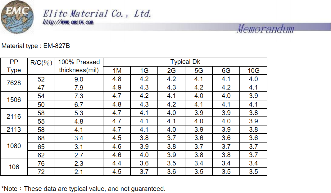
One important parameter to consider when calculating impedance is the dielectric constant. The dielectric constant for one type of material does not always have strictly one single and constant value. Thus, for a conventional fiberglass type FR4, it depends on the percentage of resin in the material. The greater the resin content, the relatively lower the dielectric constant. Conversely, the greater the percentage of glass fiber, the relatively greater the dielectric constant. For example, let’s explore parameters of EM-827B fiberglass from Elite Material on fig. 1

Fig.1 Parameters of fiberglass EM-827B.
From the data in Fig.1 it can be seen that with an increase in the operating frequency, the dielectric constant of the material tends to decrease. This feature is also important to take into account when calculating the parameters of critical conductors.
Materials from different manufacturers may differ in dielectric constant and some material characteristics, even prepregs of the same type (for example, 1080), since both the resin composition and the filler may differ.
When launching a board with impedance control, the operating frequency at which the desired impedance should be provided can be additionally specified. In this case, the manufacturer will be able not only to calculate the optimal parameters of the conductors, but also to check the compliance of the material parameters with the specified frequency. If the frequency is not specified, the factories typically test the impedance at 1 GHz.
Several parameters can be attributed to the accuracy of manufacturing: the accuracy of conductor’s width and the accuracy of gap, the thickness of the foil and dielectrics. The standard accuracy for conductor and gap detection for a foreign manufacturer is ±20%. The accuracy of foil and dielectric thicknesses in the finished board is largely determined by the thickness tolerances of the raw materials, which is typically ±10% of nominal. Fairly large tolerances for the thicknesses of the raw materials and the standard tolerance for the width of the conductors cause difficulties in providing an impedance tolerance of less than 10%.
The board structure is formed on the basis of materials with a standard range of thicknesses. The thickness of the dielectric layer, although it can be selected with a fairly small step, is not enough to accurately obtain the desired impedance values. A simple method to ensure the desired impedance values is to refine the calculation and then adjust the width of the critical conductors. If the calculations at the design stage have been performed accurately enough, then the changes that need to be made when adjusting the width of the conductors may not exceed 10% of their original value. At the request of the designer, the manufacturer can agree with him the working structure of the board and the calculated parameters of the impedance control before starting production. Many advanced PCB CAD systems, such as Cadence Allegro, provide functionality to change the routing of selected “classes” of circuits in a group way, specifying new values for the width of the conductors and the gap in the differential pair, which allows to almost instantly adjust the finished PCB design to the manufacturer’s recommendations.
When ordering boards with impedance control, some specifics of their production should be taken in account. Boards in factories are made on technological panels. Each panel accommodates the maximum possible number of boards. Impedance testing at the factory is not performed individually for each conductor on each board, but on special test coupons. The test coupon is like a small board on which the parameters of the critical conductors of the manufactured boards are modeled. It is placed on the technological fields of the factory panel, usually one test coupon per panel. The test coupon, located at the edge of the panel, is in the most unfavorable conditions in terms of maintaining the geometry of the conductors and gaps. Thus, if the impedances of the conductors located on the test coupon correspond to the specified ones, then the impedances of the conductors of all boards on the factory technological panel correspond to the specified values as well. Of course, the test coupon occupies some useful area of the factory panel, so it can fit fewer printed circuit boards than usual. This leads to a rise in price by 3-5% in the serial production of boards with impedance control.

Fig. 2a Example of a test coupon for impedance control

Fig.2b Contact pads on the test coupon, for performing an impedance test using the TDR method
Once corrected conductor widths and clearances have been determined, the necessary changes must be made to the manufacturing data. The width of each type of conductor requiring impedance control must be adjusted according to the previously calculated design value.
In this regard, it is important to understand some of the features caused by implementation of the conductor width correction in production:
- The manufacturer accepts projects mainly in Gerber RS-274-X format (with built-in aperture description) plus drilling in Excellon format. The Gerber format does not support information about circuits and their names in the source project. For this reason, the impedance requirements specified as a list of circuit names of the original design will not be entirely correct from the point of view of production, since the source data contains information in an inconvenient or unsupported form for the Gerber format.
- The PCB preparation software used in factories mainly work with such properties of graphical objects as object type, shape and size. Such parameter as the “D-code” of a graphic object (that is, “aperture” or “flare” for a photoplotter in Gerber files) is almost unavailable for work and is not used. This means that if conductors of different types, such as single conductors and diff pairs, are drawn with lines with different D-code numbers, but have the same geometric shape and size, the manufacturer will not be able to distinguish conductors of one type from conductors of another type. For example, it is not possible to distinguish between 0.1 mm single conductors, 0.1/0.1 mm diff pairs and 0.1/0.12 mm diff pairs and individually optimize their width at the factory. This means that for several types of conductors simultaneously it will be possible to achieve impedances that are only close to the nominal values, but not exactly corresponding to them. Setting the parameters and design impedances for one type of conductor will cause the impedances of other types of conductors to deviate, and vice versa.
The factors described make it difficult to achieve the specified impedance values and the specified accuracy when manufacturing boards at the factory. They, in turn, are closely related to such an important group of factors, which can be conditionally called “the influence of project features”.
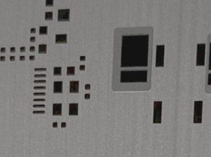
In many printed circuit board designs that come to our company for manufacturing, there are often features in the routing that affect the deviation of impedances from nominal values. Some of them look like design errors, rather than done by developer on purpose. For example, in some cases, circuits that require impedance control are made without a screen polygon in some sections (see Fig. 3).

Fig.3 An example of incorrect shielding (lack of a reference layer) for individual sections of diff-pairs, found when viewing Gerber files before ordering the production of the board (CAM350 package).
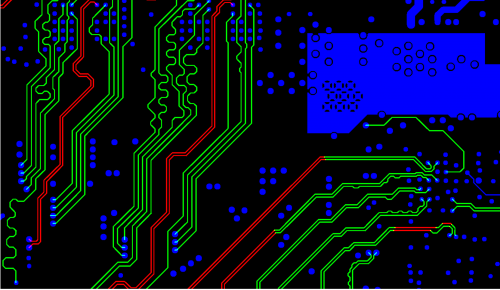
It is clear that the width of the conductors and the gap in the differential pairs, with the exception of individual bottlenecks, must strictly correspond to the specified nominal values. Otherwise, local impedance changes can create unacceptable signal distortion. However, in some projects there are diff-pairs with different conductor widths or gaps in different areas (Fig. 4).

Fig.4 Examples of diff-pairs with different conductor widths in different sections.a) Unit conductors 0.112 mm, diffuse pairs 0.11/0.14 with 0.112/0.14 mm

b) diff-pairs 0.11/0.14 with sections of 0.112/0.14 mm and differential pairs 0.127/0.127 mm with a section of 0.112/0.127 mm
Sometimes there are projects with noticeably different gaps in different parts of the diff-pairs, see Fig.5.
Different gaps in differential pairs do not contribute to high accuracy when providing impedance. In this case, diff-pairs obviously require clearance correction before manufacturing. Without this, making a board with even a minimal impedance tolerance is unlikely to save the situation.

Fig.5 An example of diff-pairs with different gaps between conductors in different sections
This phenomenon is not always caused by the developer’s carelessness. Some design programs themselves allow small deviations from the nominal gap (for example, Altium P-CAD200x programs slightly increase the gaps of diff-pairs on diagonal sections).
Also, deviations in the gap of diff-pairs can occur when generating Gerber files for production, when a project generated in millimeters is transferred to Gerber in inch format with low accuracy of coordinates after the decimal point. Deviations may seem relatively small, but in some cases even they can cause noticeable deviations of the calculated impedance values from the nominal ones.
Another important factor influencing impedance deviations is the inhomogeneity of the dielectric structure, consisting of intertwined glass filaments and resin. One conductor may be located above the glass filament in the dielectric, and the next one may be located above the area where the resin is predominantly located. The dielectric constant of the resin and glass differ by more than 30%, and this leads, firstly, to an impedance deviation, and secondly, to phase delays in the differential pair (in one arm of the differential pair, the signal will propagate more slowly than in the other). At signal speeds greater than 1 Gbps, this factor can lead to serious problems. In order to reduce its influence, developers use dielectric materials with denser fiberglass weaving, and also use diagonal placement of conductors – in this case, due to the departure from the horizontal and vertical, along which the weaving of glass filaments is located, the impedance is “averaged” along the length conductor.
Conclusion:
The actual characteristic impedance of the conductors on the printed circuit board does not always match the pre-calculated or factory-measured values. Calculated with high accuracy, the calculated impedance values can be obtained with deviations, both due to the design features and due to manufacturing inaccuracies. Simply reducing the impedance tolerance when ordering the board fabrication may not produce the expected result. The best board impedance results can be achieved by a combination of high-quality workmanship and careful routing. In critical cases for boards, preliminary signal integrity modeling can be applied, for example, in systems such as Sigrity and similar.
A standard deviation of ±10% of the calculated value is, in most cases, an acceptable result of impedance controlled boards.
PCB manufacturer recommendations for ordering boards with impedance control:
Conductors requiring impedance control, located on the same conductive layer, but belonging to different circuit classes (single conductors and diff-pairs, diff-pairs (1) and diff-pairs (2)), must differ in width by at least 1 µm . This will allow the manufacturer to most accurately select the optimal design parameters for each class of circuits at the plant, regardless of other classes.
Project gerber files submitted to production should, if possible, have the maximum coordinate accuracy of graphical objects that the design package can allow. The highest accuracy of coordinate transmission can be achieved by working in millimeters. For projects designed in millimeters, the recommended coordinate accuracy is “4:4” (four decimal places minimum) or “4:5”. In inches, the accuracy of the coordinates can be “2:5” or “3:6”.
A decrease in the effect of conductor width deviations on their impedance is achieved by increasing their width and increasing the thickness of dielectrics. Conversely, when the dielectric thickness is reduced to 0.1 mm or less, even a small deviation in the conductor width can lead to noticeable changes in impedance. For circuits requiring maximum impedance accuracy, it can be recommended to use a dielectric thickness up to the reference layer of 0.15-0.2 mm minimum.
In cases where it is required to increase the thickness of the dielectric from the microstrip line to the reference layer, but the structure of the multilayer printed circuit board does not allow this, you can locally, only under the required microstrip lines in the Top layer, make the reference layer not in layer 2, but in layer 3 or 4, thus freeing intermediate layers from tracing and copper polygons. In this case, it is necessary to add to the manufacturer that a different reference layer is selected for the conductors in the area, and an additional prohibition is added to add topology elements in this area in intermediate layers. Otherwise, the manufacturer may voluntarily add process copper fill in the empty areas of the inner layers, which can lead to signal integrity problems in the finished electronic assembly.
When transferring the project to the manufacturer, we recommend to accompany it not only with the layer structure indicating the thicknesses of the dielectric and copper, but also with a table describing the requirements for the impedance of conductors. In this table, for each “class” of conductors with impedance control, the following parameters should be indicated:
- Layer number
- Conductor width
- Conductor width and gap if it is a differential pair
- Reference layers for this type of conductors
- Required impedance
- Impedance tolerance
- Comments and features
An example of a PCB impedance requirement description is shown in Table 2. The top layer has 0.155 mm wide conductors with an impedance of 50 ohms relative to reference layer 2, with a tolerance requirement of 10%. There are also differential pairs with 0.1 mm conductors and 0.15 mm gap, with an impedance of 100 ohms. In addition, on both sides of the board there are microwave microstrip lines 0.48 mm wide with an impedance of 50 Ω relative to reference layer 3. Below these microstrips in the design, there should be no copper in the adjacent layer, and there should be an analog ground polygon in the third layer relative to the surface. Due to the increased width of the conductor, it is possible to increase the accuracy of the width of these lines, and therefore improve the impedance tolerances from 10% to 7%. A comment has been added to the table, prohibiting the placement of technological copper fillings in this area of the board. There are also 0.127 mm wide conductors in layer 3, with support layers in layers 2 and 4, having an impedance of 50 ohms.
Table 2. An example of a specification for the manufacture of a printed circuit board with impedance control.
| Layer | Conductor width, mm | Gap of differential pair, mm | Impedance, Ohm | Reference layers | Admittance | Comments |
| Top | 0.155 | 50 | 2 | 10% | ||
| Top | 0.105 | 0.17 | 100 | 2 | 10% | |
| Top | 0.48 | 50 | 3 | 7% | Do not copper fill layer 2 under these conductors | |
| 3 | 0.127 | 50 | 2, 4 | 10% | ||
| Bottom | 0.48 | 50 | 6 | 7% | Do not copper fill layer 7 under these conductors |
Providing such a table when ordering printed circuit boards will allow the board manufacturer to clearly define which conductors should be checked, and also allow them to be “fine-tuned” in width or layer structure, in order to optimally meet impedance requirements.
An example of calculating the impedance of conductors for such a printed circuit board in OrCAD Standard PCB CAD is shown in Fig.6. In this calculation, we did not set the exact values of the dielectric constant separately for each layer, setting everywhere the approximate “preliminary” value of 4.0, which is common for typical FR4 dielectrics. Later, the board manufacturer can refine these values separately for each layer, depending on the type of prepregs chosen and the material brand

Fig.6. An example of calculating impedances on a printed circuit board (CAD OrCAD Standard)
Note that the structure turned out to be “as if” asymmetric in terms of the placement of the Conductor and Plane layers, since this was required to calculate the microstrip line on the Bottom layer with the reference layer 6, and we assigned the Plane type to layer 6 and the Conductor type to layer 7, which was required for the correct calculation. But basically, the location of these microstrip lines can be limited to only some areas on the board, and in other areas we can place digital ground polygons in layer 7, which ensures the symmetry of the structure (symmetrical copper pouring of layer 2 and layer 7) and improves the quality of the printed circuit board. improving its flatness.
Thanks for your blog, nice to read. Do not stop.