Allegro Options
The main feature of the Cadence Allegro product line is the ability to expand capabilities through plug-ins. Each plug-in option is dedicated to a specific task and provides additional functionality for the PCB design process.
- High-Speed option
- Miniaturization option
- Symphony Team Design
- Manufacturing option
- Analog/RF option
- OrCAD / Allegro Productivity Toolbox
- Design Planning option
- ASIC prototyping with FPGA’s
High-Speed – work with high-speed interfaces
This option was included into the Allegro Venture license and cannot be purchased separately anymore.
This option significantly expands the functionality and automates some of the routing steps for high-speed digital printed circuit boards. It contains tools such as:

Timing vision – color differentiation of transmission lines in a group according to their relation to the TARGET transmisison line during delay tuning.
Auto-interactive delay tune – a tool for automatically aligning the lengths of transmission lines within a group of signals.
Auto-interactive phase tune – helps to automatically equalize the dynamic phase in differential pairs.

Return path VIA – automatic addition of return curent ground VIAs when signal transitions from layer to layer. First, the user selects the desired GND via pattern.
Second, once the signal routing parameters are defined, VIAs with the desired location and properties are added to the board.
Scribble routing – allows you to trace with strokes, marking only the approximate location of the path of conductors.
Snake routing – allows you to lay conductors by pressing them to the pads. With this laying method, the maximum available space is freed up for the next conductor.
To find out about other useful features in the High-speed option, ask our engineers by e-mail.
Miniaturization option
This option is available inside the Allegro Venture license and cannot be purchased separately anymore.
This option allows the use of discrete components built into the PCB body (Embedded Components). Also it adds the functionality of HDI via structures (HDI – High Density Interconnect).


In the Constraint Manager rule editor, the Micro VIA object and clearance control section are added to the new object type. Micro VIAs can be stacked on top of each other. The user sets the rules of relative positioning. Functionality for editing the Micro VIA view is added. With a single click, multiple Micro VIAs are added to change from the active layer to the specified one, if this cannot be done with a single hole.
Functionality of Embedded Components:
- Automatic creation of cavities with parameters defined in the PCB stackup settings.
- Support for active and passive components.
- Direct or indirect connecting technology for built-in components.
- Performing DRC checks for size and gaps between cavities.
Symphony Team Design
This option is purchased separately and can be used with Allegro PCB Designer and Allegro Venture licenses.
It allows several engineering team members to work on the same PCB design at the same time. The PCB design resides on a server, and all collaborators connect to it via the network. When any object on the printed circuit board is edited by one of the participants, the other PCB layout engineers see it as locked and cannot change it. The ban on changing the object is valid until the end of the actions of the first engineer on this object.
Manufacturing option
This option is purchased separately and can be used with Allegro PCB Designer and Allegro Venture licenses.
The option includes three tools at once:
- Documentation Editor
- Panel Editor
- DFM Checker
For OrCAD users, it is possible to purchase each tool separately, but the functionality of OrCAD tools is slightly reduced.
OrCAD® Documentation Editor – a PCB design document editor that intelligently automates the process of creating your design documents so you can design PCB design documentation in a fraction of the time it normally takes. Executed as a typical Windows application, OrCAD Documentation Editor allows you to quickly create production drawings that are transferred to PCB manufacturing, assembly, archiving and accompanying the product in production. All requirements of particular standard can be taken into account when creating a CD in OrCAD Documentation Editor, including stamp and frame templates, various fonts, special symbols, callouts, etc.
OrCAD® Panel Editor – a multiboard panel editor that intelligently automates the panel definition and documentation process to design simple or complex PCB panels in less time than traditional manual methods. Intuitively designed, the OrCAD Panel Editor allows you to quickly design your panel and create production drawings that are passed on to PCB fabrication and assembly.
Using imported PCB design data from OrCAD, automatically create a multiplied panel (copy with repetition) of a PCB in a production drawing. Quickly place top, bottom, drill, or custom panel layouts on a drawing, and create drill tables, note and specification lists, milling and scribing drawings.
Drilling and callout tables created at the panel level reflect the location of all PCBs on the panel and define all components, hole sizes, locations, symbols, and quantities based on the panel as a whole. You can quickly take into account design changes (ECO) by updating only the original data in CAD, since all elements of the drawing remain linked to this original data when creating new versions.
Import CAD data to drive the panel documentation generation process, while additional external content can be imported and embedded in drawings independently. The panel design program uses the available PCB and milling data to automatically assign a milling program to all boards in the panel.
OrCAD® DFM Checker provides a comprehensive yet easy-to-use PCB manufacturing analysis technology that identifies specific design issues that can have a negative effect on PCB manufacturing.
Designs that successfully pass verification against standard DRC rules may still contain critical issues that can result in poor fabrication or assembly yields, or costly rejection and delivery delays. The DFM Checker tool allows you to correct potential production issues before the design is sent to your PCB manufacturer to prevent delays in production and, as a result, in the release of the finished product to the market.
Powerful, yet easy to use, manufacturing analysis for simple and complex designs. The analysis is presented as a diagram, which allows you to quickly find the root of the problem Millions of DFM checks and the analysis process itself can be easily controlled by you by creating sets of rules organized by layer types and subcategories.
Identify issues in your design that could potentially result in low PCB fabrication or assembly yields, or costly scrap. Define, save, and reload the type and order of checks to be made. Cross-probes and DRC markers provide visualization of DFM analysis errors directly in the OrCAD PCB Editor.
Analog/RF option
This option can be purchased in addition to the Allegro PCB Designer (ALG200) license and to the Allegro Venture (ALG300) license.
This option is an additional toolkit that allows you to use parameterizable RF components both in the DE HDL/OrCAD Capture schematic editor and in the PCB canvas. The bidirectional exchange of parameterizable data makes it possible to transfer information both from the circuit design to the printed circuit board topology and vice versa.
You can create your own RF structures and store them in the component library.

It is possible to transfer parts of the design to Keysight® ADS simulation environment.
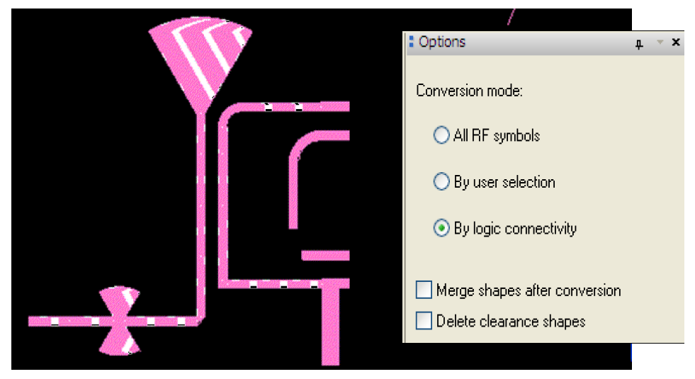
Since the Analog/RF option supports parameterized topological microwave elements, it provides a very simple mechanism for creating, placing and connecting microwave elements on the board. It allows you to easily route striplines and microstrip lines with various turning options, such as “optimally beveled” microwave corner, rounded or rectangular corner. It also allows you to directly connect two points with a RF path or a meander with specified properties.
Other features for tracing RF boards include:
- Moving, rotating, mirroring, copying selected RF components or groups of objects (polygons, lines, topological elements, vias)
- Bulk copy, flip, rotate RF components or sets
- Transfer of RF components or their groups from layer to layer
- Changing the parameters of objects and automatic regeneration of their shape in accordance with the new parameters
- Inserting library microwave components during routing
- Electrical calculations and indication of microwave path parameters
- Creating your own topological RF elements
- Converting microwave elements to polygons
- Converting Allegro traces (conductors) to stripline transmission lines
- Chamfering at the corners of microwave paths
- Indication and modification of the values of variables and expressions
- Fast multiplication of microwave fragments, including mirror reflection for symmetrical/balanced circuits
OrCAD / Allegro Productivity Toolbox
The option offers the user new tools that facilitate some additional advanced operations, useful while designing some kinds of PCBs.
The Allegro Productivity Toolbox option can be purchased in addition to the Allegro PCB Designer (ALG200) license and to the Allegro Venture (ALG300) license.
The OrCAD Productivity Toolbox has reduced set of functions, and this option can only be connected to OrCAD products.
List of productivity tools and a brief description:
| Type | Allegro Command | Description |
| Advanced Mirror | tbx advmirror | Advanced Mirror – this tool allows the user to perform the mirroring operation during copying, moving a group of objects. The mirroring operation can be performed both from layer to layer (TOP<->BOTTOM), and within one layer. (simple geometry reflection) |
| Generate Barcode | tbx barcode | Barcodes are used to record information in a machine-readable format. The Barcode Generator allows the user to place such specialized objects on the PCB. |
| Batch Plot | tbx batchplot | Allows you to combine different PDF files into one document and print multiple documents at one time. |
| CAF-DRC1,2 | tbx cafdrc | CAF-DRC allows you to reduce the risk of CAF errors using “fiber aware Hole-to-Hole” checks. |
| Change Net | tbx changenet | Allows you to change the chain affiliation of VIAs and conductive lines without rerouting them. |
| Change Width | tbx changewidth | Allows you to change the width of conductive lines and their segments without rerouting. |
| Class Color | tbx classcolor | Allows the user to colorize net classes for ease of reading, identification of ownership, and printing of traces on color printers. |
| Coil Designer1 | tbx coildes | Allows the user to create helical parameterizable inductive structures. (flat printed coils) |
| Crosscopy | tbx crosscopy | Expands copying options. |
| Custom Variable Place1 | tbx customvar place | Introduces the ability to use meta-data on PCB drawings. |
| Design Compare1 | tbx descompare | Compares two PCB designs and reports the differences found. |
| Drawing Size | tbx drawingsize | Allows you to change the size of the editable area of the project. Provides a more user-friendly interface than regular tools. |
| Highlight Dummy Pins | tbx dummypincol | Provides a list of all pins in the project that are not connected to any net. |
| Find Padstack | tbx findpadstack | Allows you to search for all padstacks in a project by their name. |
| Mask Generator1 | tbx genmask | Allows you to change the parameters of the openings of the solder mask and solder paste on the PC without the need to edit the footprints. |
| Help1 | tbx help | Shows Help. |
| Label Tune | tbx labeltune | Label Tune is an application which allows the user to improve text label readability in a more automated way. |
| Mfg Collector | tbx mfgcollect | A tool that allows you to “collect” all files for production in one place. Includes options for renaming files. |
| Net Visibility Manager | tbx netcolorview | Allows you to save and restore the visibility settings of rubber links and chain colors. Useful when planning a trace. |
| Padstack Usage Report2 | tbx padusage | Allows you to create lists of padstacks used in footprints. Extracts information from DRA files (*.dra). |
| Panelization1 | tbx panelize | Allows to simplify the process of boards panelization in the project and the output of Design Documentation. |
| Panelization1 | tbx panelize loadartwork | |
| Panelization1 | tbx panelize place | |
| PCB Library Plot | tbx pcblibplot | Allows you to print the footprints of project components as a single PDF file. |
| Polar Grid Setup | tbx polargrid setup | Allows you to use polar coordinates when working with circular PCB designs. |
| Post Processing | tbx postproc | An interface that controls the settings for the process of outputting files for production. |
| Push to Grid1 | tbx push2grid | Allows you to highlight components that do not fall into the nodes of the grid with their contact pads. Allows you to shift components to the grid nodes closest to them automatically. |
| Quick Symbol Edit | tbx quicksymedit | Allows the user to change PCB footprints without opening them in a separate window. Works similar to the command Tools – Modify Design Padstack. |
| Shape Utilities | tbx shapeutils | Contains a set of functions that make it easier to work with polygons and conductive areas in a PCB design. |
| Shield Routing1 | tbx shieldroute | Allows you to create screens over traces directly in the PCB editor. |
| Silkscreen2 | tbx silkscreen | Allows you to change the marking parameters in the entire project and carry out checks for gaps before opening from the mask. |
| Variant Assembly1 | tbx variassy | Simplifies the creation of drawings to display various PCB options. |
| Variant BOM1 | tbx varibom | Allows the user to create Pick&Place files depending on PCB options. |
| ZDRC1 | tbx zdrc | A tool that allows you to perform DRC checks on the Z axis. |
1 – Not available in OrCAD Productivity Toolbox.
2 – Not available in v16.6 and earlier versions.

Design Planning
The option exists in the Allegro basic license (ALG200) in a reduced functionality and is fully available in Venture license (ALG300).
This option allows:
- Net optimization within the group.
- Distribution of net groups by layers with color indication.
- Allows you to generate a trace exit automatically from under the BGA chip.
- Generates a trace that follows the direction of the given bundle.


ASIC prototyping with FPGA’s

The option allows you to optimize the connection of big ASIC BGA, FPGA and/or peripherals using the patented FPGA System Planner engine. Information about the possibility of swapping FPGA pins from the FPGA System Planner project is loaded into the PCB project. The pins are reconnected either manually by the engineer, or by changing the position of the microcircuits relative to each other automatically.
A typical task that this option solves is reconnecting the FPGA pins in an optimal way after rearranging the components on the PCB relative to each other. After reconnecting the pins, information can be automatically transferred from the PCB editor to the FPGA System Planner, to schematic design, and further to the FPGA code development tools.

