CAM350 – technological analysis of printed circuit board projects
The CAM350 tool is a pre-processing and design verification system designed for design engineers or process engineers who send a design to a PCB manufacturer in Gerber, ODB++ or IPC-2581 format.
CAM350 is often used in conjunction with BluePrint design documentation preparation software, but can also function as a separate product.
The system contains a huge set of design checks in terms of Design For Manufacturing (DFM), Design For Assembly (DFA), Design For Test (DFT) to detect errors and non-technological places, bottlenecks, defects, and correct them in the original PCB project. Some corrections can also be made directly in Gerber files.
The CAM350 system is not a tool for production preparation, or for more dense topology work requiring “PCB etch production area technologist” qualification, and does not provide pre-production processing functions such as “pad trimming” or “sub-etch compensation”. The program interface and feature set is as simple and easy to use as possible, while providing the design and production engineer with all the tools necessary to find and correct errors.
The advanced features of BluePrint-PCB tool integrated with CAM350 allow the design engineer to quickly and easily create a set of design documentation based on previously created templates, as well as instantly update the set of design documentation if the version or revision of the project changes.
Depending on the license purchased, CAM350 can carry out various tasks, from simple Gerber file review of the printed circuit board project, to panelization, full check of the project for compliance with the requirements and possibilities of the chosen PCB production factory, etc.
As of the beginning of 2021, two versions of CAM350 are available:
- 32x Release version of CAM350 12.2 for Windows 7 (not supported, available “as is”).
- A 64xDisplay version of CAM350 14.5 for Windows 10.
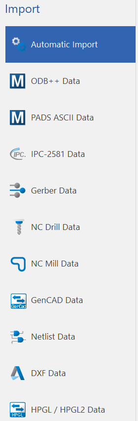
CAM350 offers the user extensive possibilities to import projects in various formats:
- Automatic information import, where CAM350 itself analyzes the files located in the directory specified by the user. During the analysis, the data format is determined and a list of files to be imported is compiled. As a result, a PCB project is created in CAM350 format.
- Import of the PCB project in ODB++ format, which includes not only Gerber and drill data, but also data about used components, list of connections, PCB stackup and other useful information.
- Direct data import from Mentor PADS ASCII format is supported.
- Import of information from IPC-2581 format, which is a standard for data exchange between electronics designers and PCB manufacturers.
- Imports graphics from PCB CAD in Gerber RS-274X file format.
- Import of PCB drill data in Exellon format.
- Uploading of milling data in the project – NC MILL Data.
- Import of graphical information such as assembly drawings or complex component housing drawings via DXF format.
- And other data import formats.
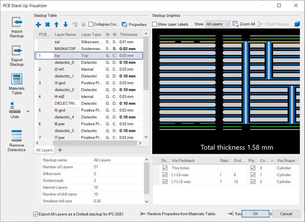
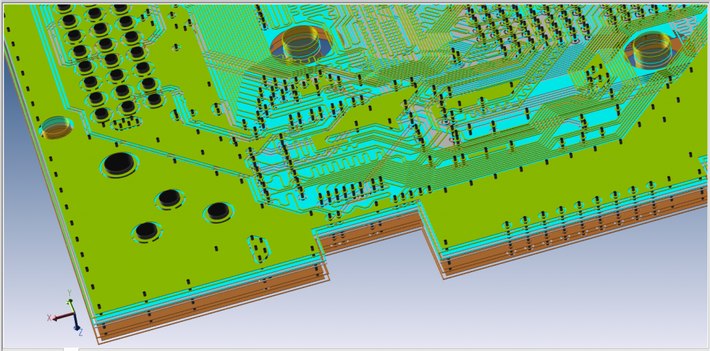
After importing information about the conductive pattern, layer order, dielectric thicknesses, etc., the user can view a visualization of the PCB stackup in 2D and 3D.
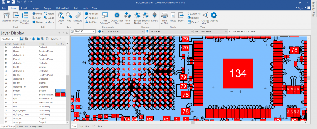
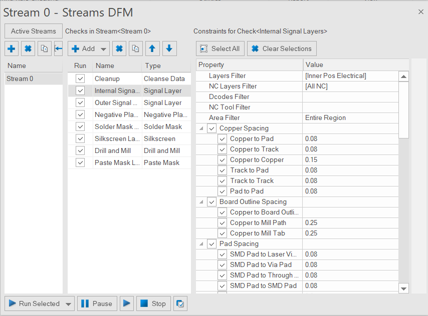
In the CAM350 it is possible to run tests in batch mode. All test settings can be stored in a separate file. Different setup files can be used for different production facilities. This makes the tests easier and faster.
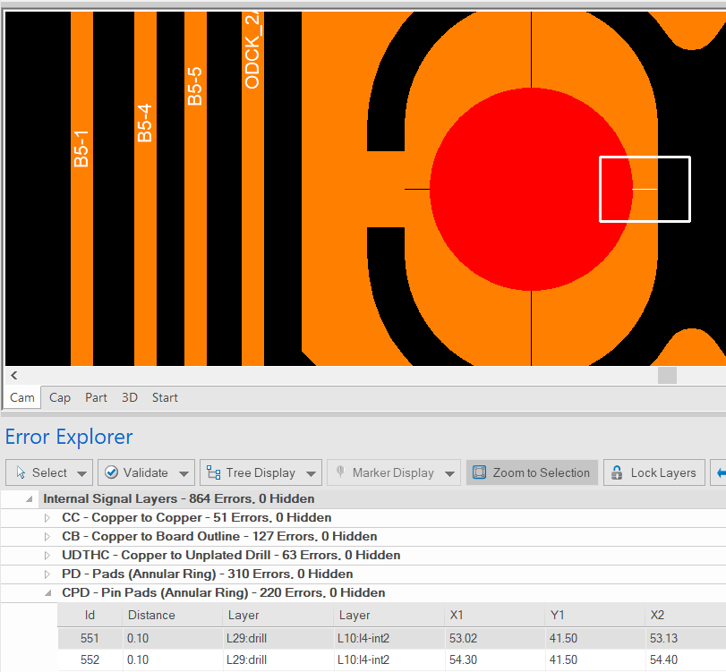
The results of DRC or DFM check are presented in tabular form. When the user selects an error of interest, the view of the project jumps to the error marker.
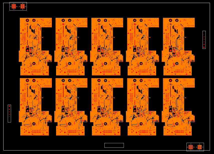
The CAM350 offers powerful capabilities for panelization of ready-to-produce PCB designs.
A short list of the most useful features of CAM350:
Friendly user interface
Customizable windows, menus, icons. All commands can be grouped as desired.
Ability to create DRC/DFM check sequences – batch mode analysis allows you to run a set of checks in the desired sequence.
Multiple layer stackup support for flex-rigid boards – the PCB designer can assign areas and set each area to a different layer stack, with appropriate mapping in 3D.
The ability to compare Gerber files of two projects – the engineer can automatically compare the initial project and the modified project received from the manufacturer of printed circuit boards after technical preparation.
Support for HDI technology, microvias, embedded components and slots – the engineer can use the latest HDI technology – microvias, blind and buried holes, embedded components and internal slots.
Database with materials – when editing the stackup of layers, the engineer can select materials from the library, as well as add the new materials.
Ability to work with negative or composite layers – the engineer has the ability to work with a layer in a “negative” format, as well as combine several layers into a composite layer (a combination of negative and positive layers). Composite layers are a very powerful tool that makes working with graphics easier.
Ability to perform DFM analysis for a specified area – an engineer can select an area with a rectangle or certain shape and run DFM or DRC analysis.
Ability to store analysis results in the project database – the user can perform a check, the results of the check are added to the project as an interactive report, and other users can view these results.
Ability to center pads relative to the master layer – the user can center the pads of a layer relative to the pads of another layer, holes, or holes relative to pads, to avoid rounding errors.
Hot link to the original PCB design – the engineer can get a report of detected errors in CAM350 and interactively navigate sequentially to each error in the original design in Allegro PCB Designer or Xpedition/PADS to make corrections, and to ensure produceability of the PCB.